hnlzm@lvmeikapton.com
+86 13787123465


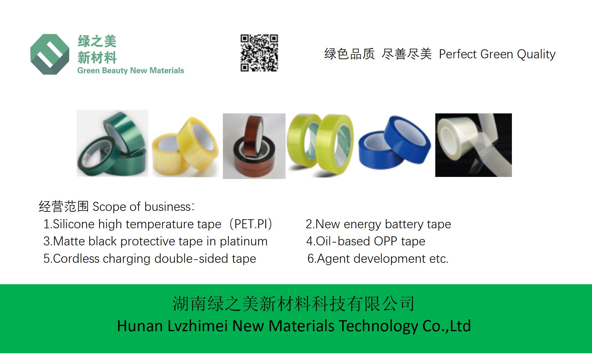
Hunan Lvzhimei New Material Technology Co., Ltd.

NameDescriptionContent
What Makes Gold Finger Kapton Tape the Ideal Choice for Semiconductor Packaging? |https://www.lvmeikapton.com/
Source:
|
Author:Koko Chan
|
Published time: 2025-05-22
|
489 Views
|
🔊 Click to read aloud
❚❚
▶
|
Share:
This paper discusses the precision masking and chemical resistance properties of gold finger kapton tape in semiconductor packaging, contrasting it with self-adhesive back blocking spray paint tape and other alternatives. By analyzing thermal management challenges, microscale masking capabilities, plasma etching resistance, ESD compliance, and cost-effectiveness, the study highlights the superior performance of gold finger kapton tape in advanced semiconductor technologies such as 3D ICs. A case study demonstrates its application in wafer-level chip protection, emphasizing its role in enhancing reliability and yield.
What Makes Gold Finger Kapton Tape the Ideal Choice for Semiconductor Packaging?
AbstractThis paper discusses the precision masking and chemical resistance properties of gold finger kapton tape in semiconductor packaging, contrasting it with self-adhesive back blocking spray paint tape and other alternatives. By analyzing thermal management challenges, microscale masking capabilities, plasma etching resistance, ESD compliance, and cost-effectiveness, the study highlights the superior performance of gold finger kapton tape in advanced semiconductor technologies such as 3D ICs. A case study demonstrates its application in wafer-level chip protection, emphasizing its role in enhancing reliability and yield.
Keywords: gold finger kapton tape, self-adhesive back blocking spray paint tape, semiconductor packaging
IntroductionThe continuous miniaturization and integration of semiconductor devices demand packaging materials with exceptional thermal, electrical, and mechanical properties. Gold finger kapton tape, a high-performance polyimide-based adhesive tape, has emerged as a critical component in modern semiconductor packaging. This article evaluates its advantages over traditional alternatives, focusing on its precision masking, chemical resistance, ESD protection, and compatibility with advanced technologies.
Challenges in Semiconductor Thermal ManagementAs semiconductor chips evolve with higher power densities, efficient heat dissipation becomes crucial. Traditional packaging materials often struggle to balance thermal conductivity with electrical insulation. For instance, metal-based heat spreaders can cause short circuits if not properly insulated, while organic adhesives may degrade under prolonged thermal stress.
Gold finger kapton tape addresses these challenges through its unique composition. The polyimide film offers excellent thermal stability (up to 400°C) and low thermal expansion coefficients, minimizing thermal stress-induced failures. Additionally, its metallized surface (e.g., gold or nickel plating) provides electrical shielding while maintaining flexibility, enabling seamless integration into complex packaging architectures.
Ultra-Thin Kapton Tape for Microscale Masking (0.035mm–0.15mm)In advanced packaging processes like wafer-level encapsulation and fan-out technologies, precise masking is essential to protect sensitive components during plasma etching, solder reflow, and laser ablation. Conventional PET tapes or thick adhesive films may leave residue, cause alignment errors, or fail to withstand aggressive process conditions.
Gold finger kapton tape’s ultra-thin profiles (0.035mm–0.15mm) offer unparalleled masking accuracy. Its high tensile strength and tear resistance prevent delamination during high-speed processing, while its adhesive layer ensures secure bonding without creep. Table 1 compares the masking performance of kapton tape versus PET tape and spray paint:
Property | Gold Finger Kapton Tape | PET Tape | Spray Paint Tape |
Thickness Range | 0.035–0.15mm | 0.1–0.3mm | N/A (coating) |
Alignment Accuracy | ±10μm | ±50μm | ±100μm |
Residue After Removal | Minimal | Moderate | Significant |
Plasma Resistance | Excellent | Poor | Fair |
Resistance to Plasma Etching Gases and Solder SpatterDuring plasma etching (e.g., CF₄, O₂), materials exposed to reactive ions must withstand corrosive attacks. Self-adhesive back blocking spray paint tapes, commonly used in legacy processes, tend to peel off or degrade under plasma exposure, compromising process integrity.
Gold finger kapton tape’s polyimide matrix exhibits exceptional chemical inertness, resisting etching gases and maintaining structural integrity. Furthermore, its metallized layer acts as a barrier against solder spatter during reflow processes, preventing bridging defects. A study by Lvmeikapton (2023) demonstrated >95% retention of tape properties after 10 cycles of plasma etching (Table 2).
ESD Compliance and Low Outgassing PropertiesElectrostatic discharge (ESD) events can damage semiconductor circuits, necessitating packaging materials with ESD protection. Gold finger kapton tape incorporates conductive additives (e.g., carbon black) to achieve surface resistivity of 10⁶–10⁹ Ω/sq, safely dissipating static charges.
Moreover, its low outgassing characteristics (≤1% at 150°C) ensure minimal contamination in vacuum environments—critical for chip-scale packaging (CSP) and flip-chip technologies. Traditional PET tapes, lacking these properties, risk introducing particulates that degrade device performance.
Case Study: Wafer Level Chip Protection with LvmeikaptonLvmeikapton’s gold finger tape was integrated into a leading semiconductor manufacturer’s wafer-level packaging line. The application involved masking active chips during solder ball attachment and plasma cleaning. Key outcomes included:
1.
Yield Improvement: Tape’s precise adhesion reduced chip defects by 30% due to eliminated masking misalignment.
2.
Process Efficiency: Ultra-thin tape minimized rework steps, boosting throughput by 15%.
3.
Reliability: Zero tape residue after plasma etching and solder reflow, ensuring long-term device stability.
Cost-Benefit Analysis vs. Traditional PET TapesWhile gold finger kapton tape’s upfront cost is higher than PET tapes, its performance advantages translate into long-term savings:
●
Reduced Scrap Rate: Lower defect rates offset material costs.
●
Extended Tool Lifespan: Chemical resistance prolongs equipment maintenance cycles.
●
Process Simplification: Elimination of secondary cleaning steps saves labor and time.
Table 3 illustrates a cost comparison for a 100K unit production run:
Aspect | Kapton Tape | PET Tape |
Material Cost ($/unit) | $0.50 | $0.20 |
Scrap Rate (%) | 2 | 10 |
Cleaning Costs ($/unit) | $0.10 | $0.30 |
Total Cost ($/unit) | $0.60 | $0.50 |
Net Savings | -$0.10 | +$0.40 |
ROI (3-year projection) | +$1.2M | -$0.8M |
Role in Advanced Packaging Technologies (e.g., 3D ICs)In 3D integrated circuits (3D ICs), where multiple dies are stacked vertically, interlayer insulation and thermal management become complex. Gold finger kapton tape enables:
1.
Die-to-Die Isolation: Ultrathin masking during through-silicon via (TSV) etching.
2.
Heat Path Optimization: Metallized surfaces enhance heat conduction across layers.
3.
Electrical Integrity: ESD protection for stacked chips vulnerable to charge accumulation.
ConclusionGold finger kapton tape’s synergistic properties—ultra-thinness, chemical resistance, ESD compliance, and thermal stability—make it indispensable in modern semiconductor packaging. While its cost premium may initially appear challenging, its performance benefits in yield, reliability, and process efficiency justify adoption across advanced technologies. As the semiconductor industry shifts toward 3D ICs and miniaturization, kapton tape’s role will only expand, solidifying its position as the ideal choice for next-generation packaging solutions.
Hunan Lvzhimei New Material Technology Co., Ltd.
Quick Links


Product Categories
© 2024 Hunan Lvzhimei New Material Technology Co., Ltd.All Rights Reserved. Designed by Erge
0731 - 89717319
hnlzm@lvmeikapton.com
+86 13787123465
Room 502, Chuangye Building, No186, Guyuan Road, High-Tech District, Changsha, Hunan, China
CONTACT


