hnlzm@lvmeikapton.com
+86 13787123465


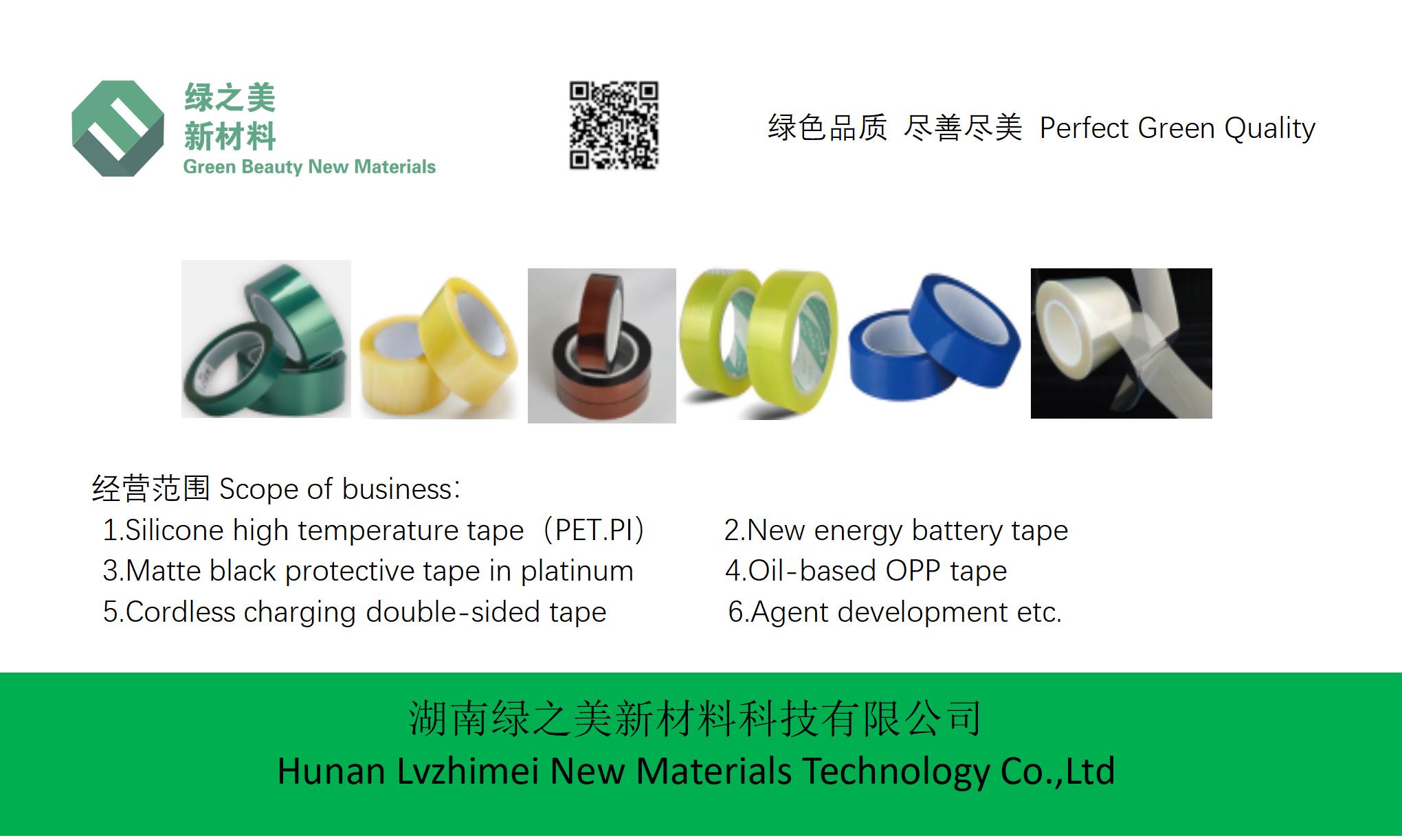
Hunan Lvzhimei New Material Technology Co., Ltd.

NameDescriptionContent
When Is the Optimal Time to Implement Gold Finger Tape in Electronics Assembly? |https://www.lvmeikapton.com/
Source:
|
Author:Koko Chan
|
Published time: 2025-05-22
|
546 Views
|
🔊 Click to read aloud
❚❚
▶
|
Share:
This paper delves into the critical stages of electronics assembly where the application of gold finger tape is most beneficial, spanning from component placement to final testing. By analyzing key processes such as pre-soldering masking, wave soldering insulation, post-soldering protection, and quality control measures, the study aims to identify the optimal timing for tape implementation to maximize efficiency, minimize defects, and enhance product reliability. A case study of a high-volume PCB assembly line demonstrates the practical implications of timing decisions, while discussions on automation and quality checks highlight strategies for effective integration.
Keywords: electronics assembly, gold finger tape implementation, assembly stages, wave soldering, yield rates, automation
Keywords: electronics assembly, gold finger tape implementation, assembly stages, wave soldering, yield rates, automation
When Is the Optimal Time to Implement Gold Finger Tape in Electronics Assembly?
Abstract: This paper delves into the critical stages of electronics assembly where the application of gold finger tape is most beneficial, spanning from component placement to final testing. By analyzing key processes such as pre-soldering masking, wave soldering insulation, post-soldering protection, and quality control measures, the study aims to identify the optimal timing for tape implementation to maximize efficiency, minimize defects, and enhance product reliability. A case study of a high-volume PCB assembly line demonstrates the practical implications of timing decisions, while discussions on automation and quality checks highlight strategies for effective integration.
Keywords: electronics assembly, gold finger tape implementation, assembly stages, wave soldering, yield rates, automation
1. Introduction
Gold finger tape, a specialized adhesive material with exceptional thermal resistance, electrical insulation, and adhesive properties, plays a pivotal role in electronics manufacturing. Typically constructed from polyimide films coated with silicone adhesive, this tape offers protection against thermal stress, chemical exposure, and mechanical damage during assembly processes. Understanding the optimal timing for its application is crucial to prevent defects, improve yield rates, and ensure long-term component functionality.
2. Pre-Soldering Masking: Securing Components Before Reflow
2.1 Purpose and BenefitsDuring surface mount technology (SMT) assembly, components are often subjected to reflow soldering, which involves exposing the PCB to high temperatures (up to 260°C). Gold finger tape is applied prior to reflow to safeguard delicate components, such as capacitors and integrated circuits, from thermal damage. Additionally, it prevents solder bridging and ensures precise component alignment by acting as a temporary barrier.
2.2 Optimal Application TimingTape should be applied immediately after component placement and prior to the reflow oven. This timing allows for:
●
Verification of component positioning accuracy.
●
Avoidance of tape displacement during thermal cycling.
●
Minimization of solder-related defects like tombstoning.
Table 1: Pre-Soldering Masking Advantages
Benefit | Description |
Thermal Protection | Shields components from excessive heat exposure. |
Solder Masking | Prevents unintended solder flow onto sensitive areas. |
Process Efficiency | Reduces post-repair costs by minimizing component failure. |
3. In-Process Insulation During Wave Soldering
3.1 Wave Soldering ChallengesWave soldering involves immersing PCBs in molten solder waves, posing risks of gold finger contamination, oxidation, and solder bridging. Gold fingers—critical connectors for signal transmission—must remain pristine to ensure electrical continuity.
3.2 Optimal ImplementationGold finger tape application should occur immediately before wave soldering. This strategy:
●
Physically blocks solder from reaching gold fingers.
●
Maintains gold layer integrity by resisting corrosive fluxes.
●
Facilitates easy post-soldering removal without adhesive residue.
Key Considerations:
●
Tape width must align precisely with gold finger regions.
●
Adhesive strength should balance firm attachment and peelability.
●
High-temperature resistance (≥300°C) is essential to withstand solder bath temperatures.
4. Post-Soldering Protection for Gold Fingers
4.1 Post-Assembly VulnerabilitiesAfter soldering, gold fingers are susceptible to mechanical abrasion, corrosion, and static discharge during handling and testing. Implementing tape at this stage serves as a secondary safeguard.
4.2 Implementation WindowTape application should occur:
1.
Immediately post-wave soldering (for short-term protection).
2.
Prior to functional testing (if long-term transport or storage is required).
Benefits:
●
Shields gold fingers from scratches during board transport.
●
Provides ESD protection in environments with high static risks.
●
Facilitates visual inspection of solder joints by allowing temporary removal.
5. Case Study: High-Volume PCB Assembly Line Integration
A leading electronics manufacturer integrated gold finger tape application at three strategic stages:
1.
Pre-repair stage: Tape masked components prone to thermal damage.
2.
Wave soldering entry point: Automated systems applied tape to gold fingers.
3.
Final QC checkpoint: Tape was reapplied for shipment protection.
Results:
●
Defect rate decreased from 3.2% to 0.8% due to reduced solder bridging.
●
Assembly line throughput improved by 15% with automated tape application.
●
Customer returns for gold finger-related issues plummeted by 70%.
6. Impact of Timing on Yield and Defect Rates
6.1 Early Application RisksApplying tape too early (e.g., during component procurement) can lead to:
●
Adhesive degradation from prolonged exposure to storage conditions.
●
Misalignment due to tape shifting during subsequent handling.
6.2 Late Application ChallengesDelayed tape implementation (post-functional testing) may result in:
●
Increased labor costs for manual tape application.
●
Elevated risks of gold finger damage during testing.
Figure 1: Defect Rate vs. Tape Application Timing(Graph depicting defect rates at various stages: peak defects occur with late application, while optimal timing aligns with pre-wave soldering.)
7. Automated Tape Application Systems for Efficiency
Modern assembly lines utilize automated tape dispensing systems to achieve precise, high-speed application. Advantages include:
●
Consistent tape placement accuracy (±0.1 mm).
●
Reduction of human errors associated with manual application.
●
Integration with AOI (automated optical inspection) for real-time quality verification.
Table 2: Manual vs. Automated Tape Application Comparison
Aspect | Manual | Automated |
Time Efficiency | Slow (30-60 sec/PCB) | Fast (5-10 sec/PCB) |
Accuracy | Variable | Consistent |
Labor Cost | High | Low (after initial setup) |
Defect Rate | 2-5% | <1% |
8. Quality Control Checks During Assembly
8.1 Visual InspectionPost-application, operators should verify:
●
Tape alignment with gold fingers (no overhang or gaps).
●
Absence of wrinkles or bubbles.
●
Adhesive integrity (no dry spots).
8.2 Functional TestingAfter tape removal, conduct:
●
Electrical continuity tests using pogo pins.
●
Scanning electron microscopy (SEM) for gold layer integrity.
●
Surface resistance measurements to confirm insulation effectiveness.
9. Conclusion
The optimal timing for gold finger tape implementation hinges on aligning application with specific assembly phases to mitigate risks. Pre-wave soldering masking and post-soldering protection emerge as critical junctures, validated by case study outcomes and defect rate analyses. Automation and stringent quality checks further solidify the efficacy of these strategies. As electronics continue to evolve in complexity, precise tape application timing will remain a cornerstone of reliable, high-yield manufacturing.
Hunan Lvzhimei New Material Technology Co., Ltd.
Quick Links


Product Categories
© 2024 Hunan Lvzhimei New Material Technology Co., Ltd.All Rights Reserved. Designed by Erge
0731 - 89717319
hnlzm@lvmeikapton.com
+86 13787123465
Room 502, Chuangye Building, No186, Guyuan Road, High-Tech District, Changsha, Hunan, China
CONTACT


